Integrated Platform Advances Photonics Testing
An integrated optoelectronic system aims to streamline high-volume testing for next-gen AI-driven data centre interconnects.

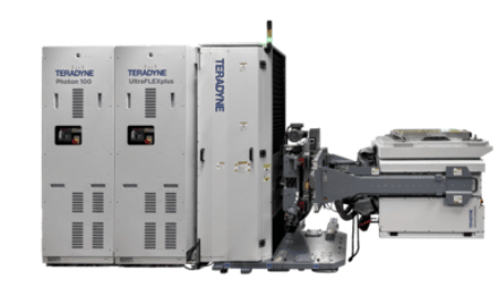
A new automated test platform from Teradyne, Inc. targets one of the biggest bottlenecks in silicon photonics (SiPh) and co-packaged optics (CPO): scaling production without sacrificing test coverage or efficiency. The system combines optical and electrical test capabilities into a single architecture to support high-throughput manufacturing across multiple insertion points.
– Advertisement –

As demand for high-speed optical interconnects accelerates, driven largely by AI workloads and hyperscale data centres, chipmakers are under pressure to transition SiPh and CPO from pilot lines to full-scale production. Traditional test setups, often fragmented across multiple vendors and tools, have made this transition complex and time-consuming.
The key features are:
- Integrated optical and electrical test instrumentation
- Supports wafer, optical engine, and CPO module testing
- Scalable architecture for high-volume manufacturing
- Customizable optical test configurations
- Open ecosystem with flexible partner integration
The newly introduced platform addresses this by integrating optical instrumentation with a proven semiconductor test architecture, enabling automated testing at the wafer level, at the optical engine stage, and during final co-packaged module assembly. This unified approach is designed to reduce operational complexity while improving throughput and consistency across manufacturing flows.
A key focus is scalability. The platform is built to handle high-volume environments, with flexibility to adapt as silicon photonics designs evolve. It also supports both standard configurations and customizable optical setups, allowing manufacturers to tailor test strategies based on specific device requirements.
Another differentiator is its open ecosystem approach. While the system provides a fully integrated solution, it still allows manufacturers to select preferred partners for probing and handling at the wafer and die levelsoffering a balance between integration and flexibility.
By consolidating multiple test functions into a single platform, the system aims to shorten time-to-market for SiPh and CPO devices while ensuring comprehensive validation. This is particularly critical as co-packaged optics gain traction in next-generation switches and AI infrastructure, where performance, power efficiency, and reliability are tightly coupled. The launch reflects a broader shift in semiconductor test strategies, where integrated, automated platforms are becoming essential to keep pace with rapidly evolving photonics-based architectures.
Click here for the original announcement.